meLab's Facilities
meLAB is currently going over a triple R process: Remodelling, Restructuring and Reorganizing.
As the dynamic research group we are, every year new students join us and with them new and exciting research opportunities come. Across all the meLAB spaces, we are listing the equipment available while making sure it is ready for operation. Considering this mission and vision, we are trying to increase efficiency, provide better services and have a greater impact on our community and society.
Our lab is equipped with several state-of-the-art tools, high-tech equipment, and high-quality processes which we have just opened to the entire research and industrial community working in medical devices, semiconductor technologies and materials processing. These facilities are here not only to support University of Glasgow students, meLAB staff and external invited guests, but also to preserve the sustainability of the group and its spaces.
Here, everyone can access and enquire about the available equipment and processes. Currently, we have 3 equipment that we are opening to the community. If you are interested in any of the below, please click on the equipment name to fill out the form and we will get back to you.
You can also access a full list of equipment and instruments below. From these, some will come available online soon, while others are readily available. Please enquire using the general contact us section of the website.

Parylene SCS Coater
SCS PDS 2010 LABCOATER is a unique system that allows to produce Parylene coatings that can be applied to components such as circuit boards, sensors, wafers, medical devices, MEMS and elastomeric components in any type of samples.
Parylene is considered by many to be the very best thin film conformal coating for environmental protection particularly in high reliability applications. Below are some typical characteristics of the Parylene C conformal coatings produce in our lab:
- Dielectric Strength – 5.600V/mil
- Dielectric Constant (60Hz) – 3.15
- Water Vapor Transmission Rate – 0.08 (90% RH, 37ºC)
- Continuous Service Temperature – 80ºC
- Thermal Conductivity at 25ºC – 0.084
For service enquiries, please fill out the form and we will get back to you shortly.

PlasmaCoat Thin Film Solutions
The PlasmaCoat is a DC magnetron sputtering apparatus used for the deposition of metallic and semiconductor thin films and complex multilayer structures which are of crucial importance for a large number of applications, including electronics, optoelectronics, and photonics.
The PlasmaCoat produces dense and uniform thin films with outstanding durability for the manufacture of single or multilayer structures over up to 3-inch wafers. Thin films obtained with this system can be utilised as dielectric layers in semiconductor devices (e.g., gate oxides in transistors), for the development of piezoelectric devices, as well-known high-k dielectric materials for power electronics, or as transparent conductive oxides.
- Max substrate size 3" wafers.
- Si and Zr targets available.
- Oxides and Nitrides based on the target materials.
- Upcoming targets: Al, Ta, Hf, Zn, ITO, and AZO.
- Room temperature depositions.
For service enquiries, please fill out the form and we will get back to you shortly.

LPKF ProtoLaser U4
The LPKF ProtoLaser U4 with integrated UV laser is capable of processing a wide variety of materials. The high pulse energy of the UV laser leads to a residue-free ablation process, resulting in geometrically precise contours.
The LPKF ProtoLaser U4 can structure or cut diverse materials quickly and cleanly. The laser wavelength used makes it a truly multifunctional tool, while it can cut individual boards out of large boards with high precision and no stress, drill holes and micro VIAS, and create openings in solder masks. It can cut and structure LTCCs, fired ceramics, ITO/TCO substrates, delicate prepregs, and laminated materials like FR4- or RF-specific substrates.
- Wide range of substrates/materials can be laser cut/etched.
- Simple operation upon design provision.
- Maximum layout area: 229 mm x 305 mm x 7 mm
- Maximum Laser power: 5.7W, structuring speed: 5.5cm³/min on laminated substrate
- Minimum line/space: 50µm/20µm on FR4 substrate
For service enquiries, please fill out the form and we will get back to you shortly.
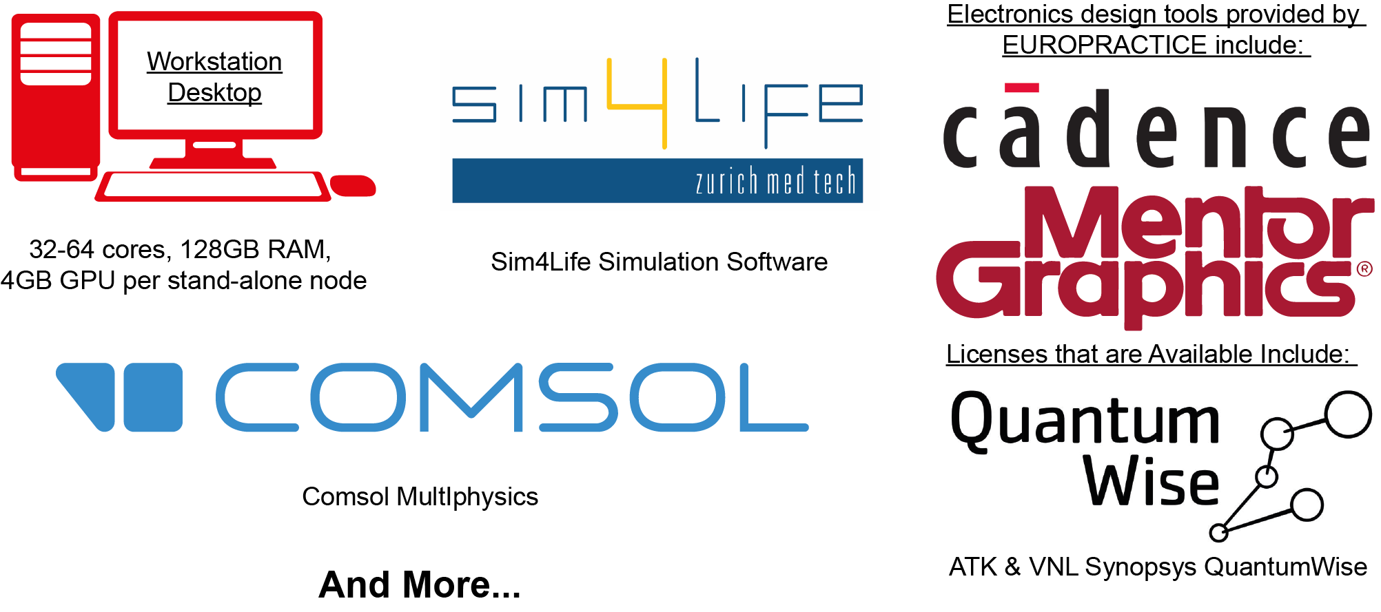
Computational Tools
Other Facilities
The meLAB is a modern Lab with tools for microelectronics design, simulation, layout and measurement from device to architecture. meLAB is affiliated with the Communications, Sensing and Imaging (CSI) group and the Centre for Medical and Industrial Ultrasonics (C-MIU) .
At meLAB, we have access to the following facilities at the University of Glasgow:
James Watt Nanofabrication Centre (JWNC) , one of the finest nanofabrication facilities in the world, featuring state-of-the-art micro/nanofabrication and metrology equipment.
Electronics Systems Design Centre (ESDC) and Kelvin Nanocharacterisation Centre (KNC) provide resources and facilities for high-end electronic, microsystem, radiofrequency, microwave, terahertz, optical, magnetic and biomedical system design, research, and development.
meLAB is equipped with state-of-the-art characterisation facilities from Tektronix:

Collaborations